Motion Mate Multi Axis Motion Controller
Description
The motion mate is designed to be somewhat of a full machine control scheme with motion control capabilities. It consists of what I like to think of as three main subsystems.
The processor subsystem is represented in blue on the block diagram. This subsystem consists of a main Digital Signal Processor that is responsible for any tasks that are not considered “real time”. What is “real time” you ask? I consider “real time” tasks to be anything that has to be synchronized to the overall system function (motor control, limit switches, e-stops, etc.) The non “real time” tasks generally consist of either handling communication protocols (USB, CAN bus, Ethernet, etc.) or doing kinematic and motion planning calculations that will be executed by the real time subsystem at a later point.
The real time subsystem is represented by green on the block diagram. This subsystem is made up of an FPGA that controls all “real time” tasks. The main “real time” tasks are providing control pulses to motor driver, synchronizing movement between Axis, and interfacing to quadrature encoders. It also handles things that an FPGA is more suited to than a DSP such as high speed I/O interfacing.
The I/O subsystem is represented by orange on the block diagram. This subsystem is less of a single system and more of many smaller systems that don’t really fit the other two subsystems. Things such as general purpose I/O that is not time sensitive, ADC and DAC interfaces for machine diagnostics, and any other “odds and ends” peripherals that may be handy for machine control.
Development progress
The below section contains info about current development status, and future development plans. Think of the info below as a checklist of what I have done, am working on, and plan for the future. Each subsystem will have a list of tasks that are require development. Tasks can consist of certain features, certain requirements of a subsystem, or just about anything that I feel is major enough to be represented by itself.
DSP subsystem
Main Component:
Texas Instruments TMS320C6748EZWT Digital Signal Processor
One C746x DSP core @ 456-MHz (3648 MIPS and 2746 MFLOPS)
448KB + Additional 128KB of on chip RAM
Dedicated DDR2 controller with 256MB Address space
361NFBGA 16mm X 16mm BGA package (19 X 19, 0.8mm pitch)
Pin to pin compatible with Texas Instruments OMAP-L138 Dual core SoC
Tasks
Complete:

PMIC
Power management IC for all power rails in the DSP subsystem

DSP Power Sequencing
Power sequence control for DSP subsystem power rails and power on reset generator

Jtag Programming and debug header
Header for XDS110 Jtag Emulator

Boot mode selection pin inputs
Inputs to the Boot mode selection pins using an octal FET bus switch

NAND Flash
4Gb (512M x 8) ONFI-Compliant NAND Flash for main program storage and boot memory

µSD Card
µSD card for boot and program storage or general file transfer to the system
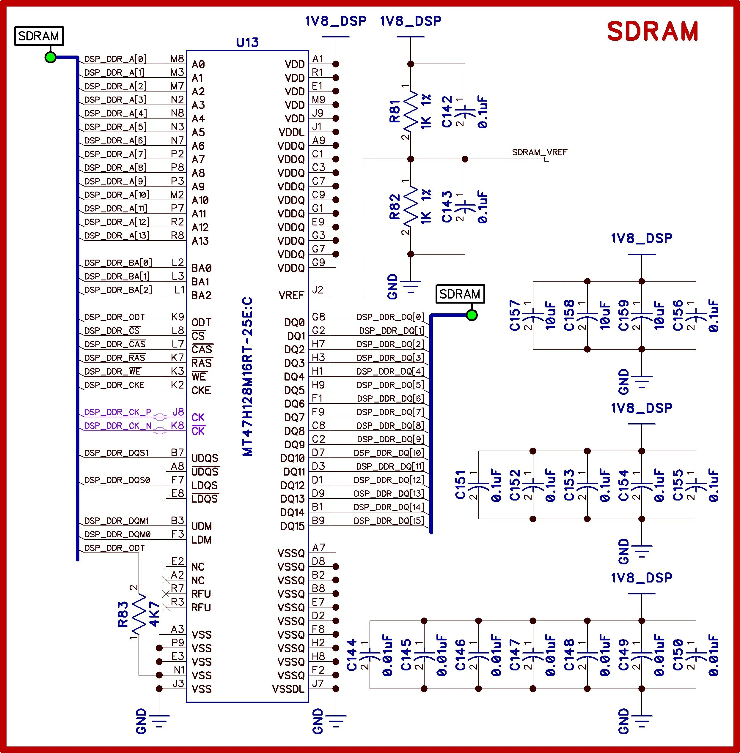
DDR2 SDRAM
256-MB of DDR2 SDRAM to act as the DSP subsystems main volatile memory

DSP Dedicated Pin Connections
All the dedicated pins of the DSP that are not power pins. Including things such as clock pins and USB.

USB On the Go
USB OTG interface to act as the main communication interface between the host PC and the DSP subsystem

Ethernet
10BASE-T/100BASE-TX Ethernet PHY connected to the DSP over an RMII interface

USB to UART interface
FTDI USB to UART IC to allow for booting from UART over a PC COM port as well as general debug/backup in case USB OTG has issues.

RS-485 interface
RS-485 interface to allow communication between the DSP and external boards for expansion options in the future.
In progress/planned:
LCD and VGA interface
DSP - FPGA interface
FPGA subsystem:
Main Component:
Lattice LFE5U-85F-8BG381I ECP5 FPGA
84,000 Logic Elements
669 Kb distributed RAM
3,744 Kb Embedded Memory
156 18 x 18 Multipliers
381caBGA 17mm X 17mm BGA package (20 X 20, 0.8mm Pitch)
Tasks
Complete:
In progress/planned:
Power circuitry
Programming interface and boot mode selection
Isolated encoder input
Isolated step/dir outputs
Limit switch interface
I/O subsystem:
Main Component:
N/A
Tasks
Complete:
In progress/planned:
Power input and board wide power circuitry
Isolated low speed and high speed GPIO
ADC
DAC
Solid state relays
Other industrial interfaces